将纳米尺度的材料(例如纳米颗粒)有序组装,是实现其特定功能应用的关键。蒸发自组装是其中易于实现、成本低、可大规模操作的一种方法。然而由于液体蒸发时内部不稳定,组装结果多为耗散结构,缺乏有序性。传统的控制蒸发自组装的方法可以使所成结构有序化,然而这些结构尺寸多在纳米尺度以上。
微波作为一种非传统加热源,已被广泛用于纳米材料的合成。相比于传统加热手段,微波具有迅速、高效、可选择性加热、均匀致热等优点。然而,将微波作为以纳米材料为基元的组装调控手段,鲜有报道。因此,研究微波场下的胶体纳米颗粒的组装行为,具有重要的理论意义和实际应用价值。
本文围绕利用微波辐照结合限定几何结构开展调控水溶剂胶体纳米颗粒的蒸发自组装的研究,主要做了以下几方面工作:
1.引入球面/平面的限定几何结构,结合微波场调控液滴蒸发时内部毛细流以及三相线的运动行为,使用以水相聚乙烯醇为稳定剂的纳米银颗粒做基础模块(building block),由于三相线做规则的“粘滞-滑动”运动,随三相线向球面/平面蒸发收缩,边缘形成了梯度同心环状组装结构。通过调控水相胶体银的浓度以及微波输出功率,可以改变环宽度、高度以及环间距;
2.为进一步抑制影响规则同心环形成的“雷利-伯纳德”涡流,引入树脂器皿,使胶体在微波下蒸发时其周围有更大的蒸汽压;实验发现,环形组装结构更趋于规整,并且蒸发过程中液滴环境蒸汽压如果接近饱和蒸汽压,微米级的环之间会形成纳米环;基于液滴半月面区域内的“滞流”原理,我们分析了这种纳米环的成因。
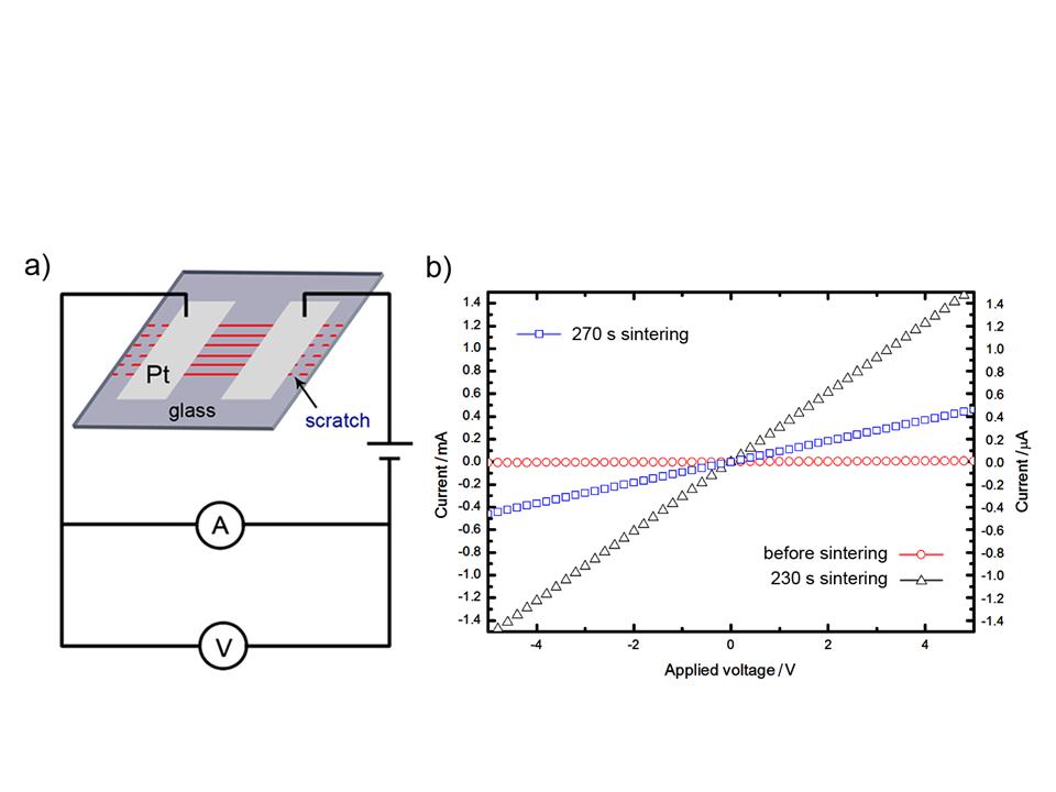
3.利用微波辅助蒸发自组装得到的纳米银颗粒组装结构,测其电学性质。伏安特性响应表明,这种组装结构具有电阻特性;为进一步降低其电阻率,我们尝试了高功率下对其进行微波烧结,结果表明微波辅助蒸发自组装结合微波烧结,有望一步制造基于电学性质的生物大分子、化学分子以及气体的微纳传感器。
G Yang, Y W Zhou, Z R Guo, Y Wan, Q Ding, T T Bai, C L Wang and N Gu*.Microwave-assisted one-step patterning of aqueous colloidal silver. Nanotechnology, 2012,23(26) 265302
Figure 1. Schematic illustration of AgNPs assembling into gradient concentric rings. (a) The experimental set-up: A drop of colloidal silver was trapped in a sphere-on-flat geometry, forming a capillary bridge. Under microwave irradiation, as the solvent evaporated, the initial AgNPs ring was deposited at the perimeter of the droplet (denoted as the red circle). “X” is defined as the radical distance away from the sphere/glass contact centre. (b) Stepwise representation of the formation of gradient concentric rings propagating from the capillary edge to the sphere/glass contact centre during solvent evaporation (top view).
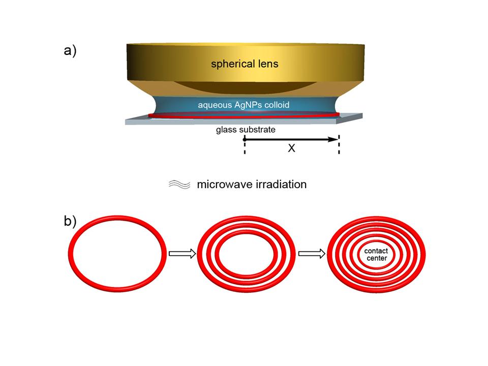
Figure 2. Optical microscopic picture of the gradient concentric AgNPs rings. The local power density of the applied microwave irradiation was 120 . The white arrow indicates the receding direction of the contact line. The scale bar is 100 .
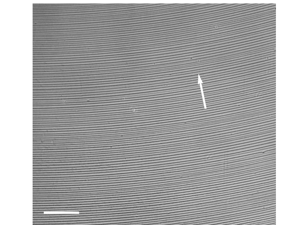
Figure 3. AFM height images of the surface patterns formed on the glass substrate at different radical positions as the contact line progressively approaching the centre of the sphere/glass contact with (a-c) 40 , (d-f) 80 and (g-i) 120 microwave. The scale bar is 10 for all images. The Z scale is 220 nm for a), 150 nm for d), 100 nm for g), 80 nm for b) and c),70 nm for e) and h), and 50 nm for f) and i).
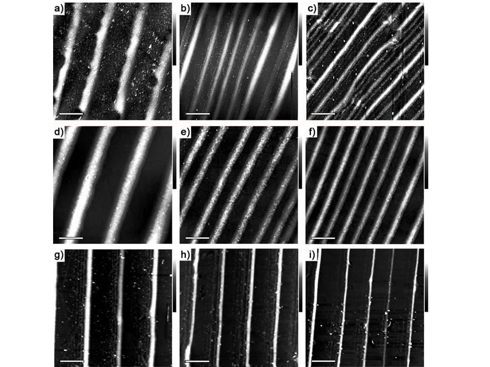
Figure 4. Optical microscopic images of the patterns formed from the EISA of the aqueous colloidal silver in the confined geometry without microwave irradiation. (a) Evaporated at the room temperature (25 ), only a single ring was deposited at the initial pinning position. (b) When heating from the bottom (~70 ), irregular multi-rings were obtained due to the temperature gradient driven hydrodynamic convective flow within the drying droplet. The scale bar is 100 for both images. The white arrow indicates the receding direction of the contact line.
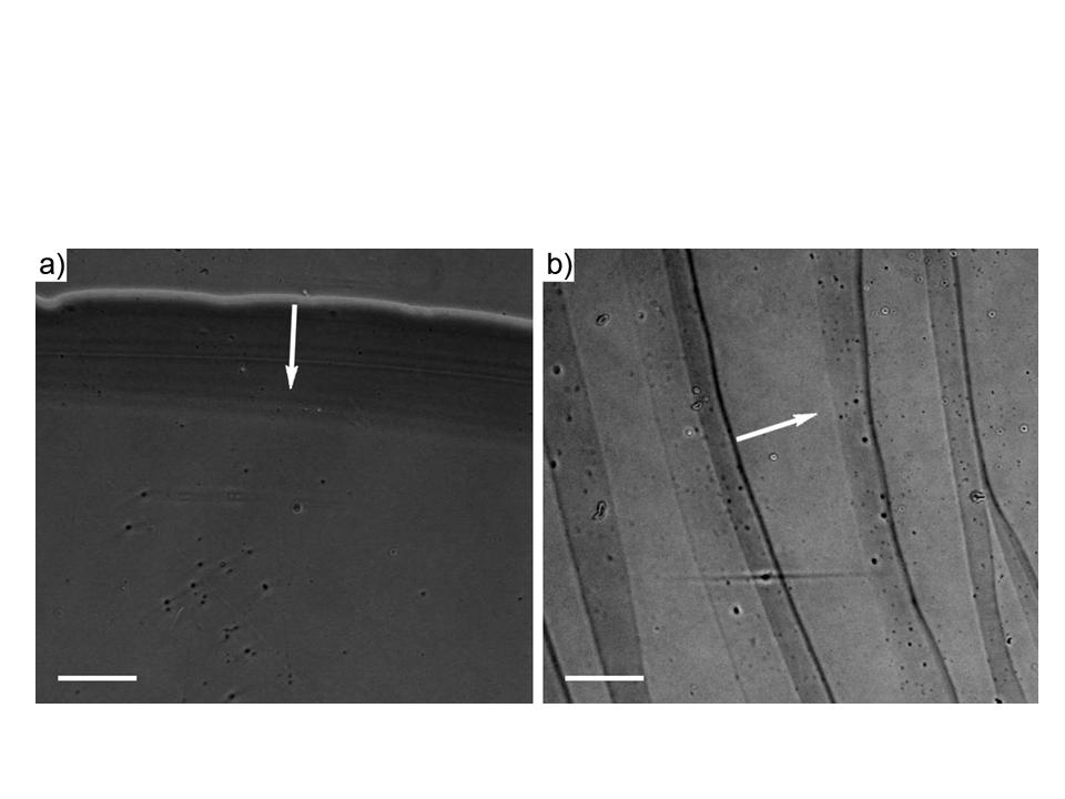
Figure 5. (a) Schematic illustration of the interspaced nanoscale rings formation within two adjacent micro rings. At the capillary edge, the internal ring has been deposited at the next pinning position before the contact line ‘slips’ (left panel). A wedge like water thin film (dashed yellow frame) is trapped because of the pre-deposited ring when the contact line moves to the next pinning position (middle panel). As evaporating, the wedge like water film goes through ‘stick-slip’ cycles to leave nanoscale interspaced rings (right panel). (b-d) A set of SEM images of the surface patterns as the contact line progressively shrinking to the centre of the sphere/glass contact. The scale bar is 10 for b) and 5 c) and d). (e-g) SEM images of detailed structure of interspaced nanoscale rings at the corresponding positions marked with black open square at b-d). The scale bar is 500 nm for e) and f) and 100 nm for g).
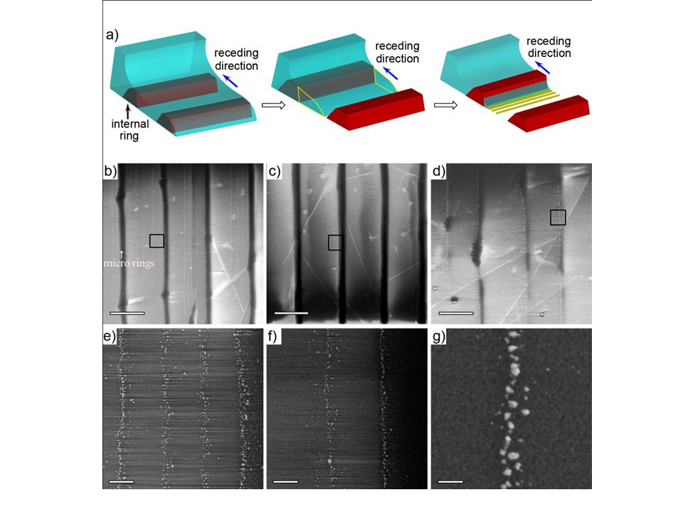
Figure 6. Electric properties measurements of AgNPs rings. (a) Schematic illustration of conductance measurement for periodic AgNPs rings. (b) Current-voltage response of the AgNPs rings before sintering (red open circles), 230 s microwave sintering (black open triangles) and 270 s microwave sintering (blue open squares).
